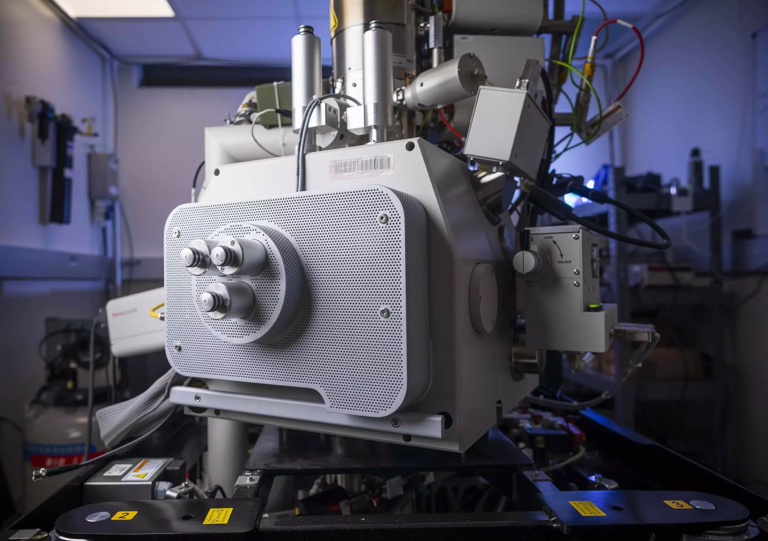
The field of semiconductor research is perpetually evolving, driven by a need for greater efficiency and performance in electronic devices. Recent developments at UC Santa Barbara (UCSB) have taken a remarkable step forward, enabling researchers to visualize the behavior of electric charges moving across the interface of semiconductor materials for the first time. This innovation not only enriches the study of semiconductor theory but also has the potential to redefine how we understand and utilize these materials in cutting-edge technologies.
When sunlight hits a solar cell, it generates charge carriers—electrons and holes—that are essential for electricity production. However, these hot carriers, excited to high energy states, lose a significant amount of energy in mere picoseconds (trillionths of a second), and conventional solar cells only capture a fraction of this energy. The investigation into hot carriers is pivotal for improving the efficiency of photovoltaic systems, and understanding their behavior in semiconductor materials, especially at heterojunctions, is critical for enhancing performance.
Heterojunctions—interfaces between different semiconductor materials—are crucial for the design of various electronic devices, ranging from lasers and sensors to photovoltaic cells. The characteristics of these interfaces can significantly affect the mobility and effectiveness of charge carriers. Using traditional indirect measurement methods has provided theoretical insights, but they have fallen short in providing direct, visual evidence of how these carriers behave when they are most energetic and thus most difficult to capture.
Researchers led by Professor Bolin Liao at UCSB utilized an innovative technique known as scanning ultrafast electron microscopy (SUEM) to directly observe the diffusion of hot carriers across a silicon-germanium heterojunction. By leveraging ultrafast laser pulses as a picosecond-scale shutter, the team was able to synchronize an electron beam with the rapid movements of these energetic charges.
Liao emphasizes that “what we’re talking about are events happening within this picosecond to nanosecond time window.” This time frame is crucial because it encapsulates the dynamic behavior of hottest carriers just after they are excited. This research not only serves to benchmark established semiconductor theories but also challenges existing paradigms by providing clear visualizations of charge transfer phenomena that were previously understood only indirectly.
The team’s findings reveal insights that are both expected and surprising. When hot carriers are generated in homogenous regions of silicon or germanium, they initially display high speeds due to their elevated energy state. However, as they approach the junction, many of these carriers become trapped by the junction potential, experiencing a dramatic decrease in mobility. This trapping effect can negatively impact the overall performance of devices that depend on efficient charge separation and collection, such as solar cells and sensors.
Liao notes the unexpected nature of their findings: “We didn’t expect to be able to image this effect directly.” This realization underscores the importance of visual evidence in semiconductor research, moving beyond theoretical models to tangible data that reveals the real behaviors of these materials in practical applications.
The significance of this research extends beyond academic curiosity. By providing a method to experimentally visualize hot carrier dynamics, Liao and his team are laying the groundwork for improving semiconductor devices. This could pave the way for more efficient energy harvesting systems, advanced electronic communication technologies, and improved sensing systems, all of which rely on effective charge carrier management.
Moreover, the research connects back to the foundational ideas proposed by UCSB’s late Professor Herb Kroemer, who championed the concept that “the interface is the device.” This new ability to visualize the junction interface in real time ties back to Kroemer’s vision and offers an exciting frontier for exploration and innovation in electronic device design.
The pioneering work of the UCSB team presents a remarkable leap forward in semiconductor research, crucially enhancing our understanding of hot carrier dynamics through direct observation. As we embark on a new era defined by greater energy efficiency and technological capabilities, this research promises to impact various fields, from renewable energy to advanced microelectronics. By illuminating previously invisible processes, researchers are not only validating existing theories but also unlocking new pathways for innovation in semiconductor technology.

