The rapid advancements in nanotechnology have spotlighted the potential of extremely thin materials, also known as two-dimensional (2D) materials, which consist of a few atomic layers. These materials have become focal points in electronics and quantum technology due to their unique properties that deviate significantly from traditional bulk crystals. As researchers explore the optical and electronic characteristics of these materials, the implications for future technologies are profound. One of the most exciting developments originates from an international research initiative led by TU Dresden, marking a significant breakthrough in manipulating excitonic states.
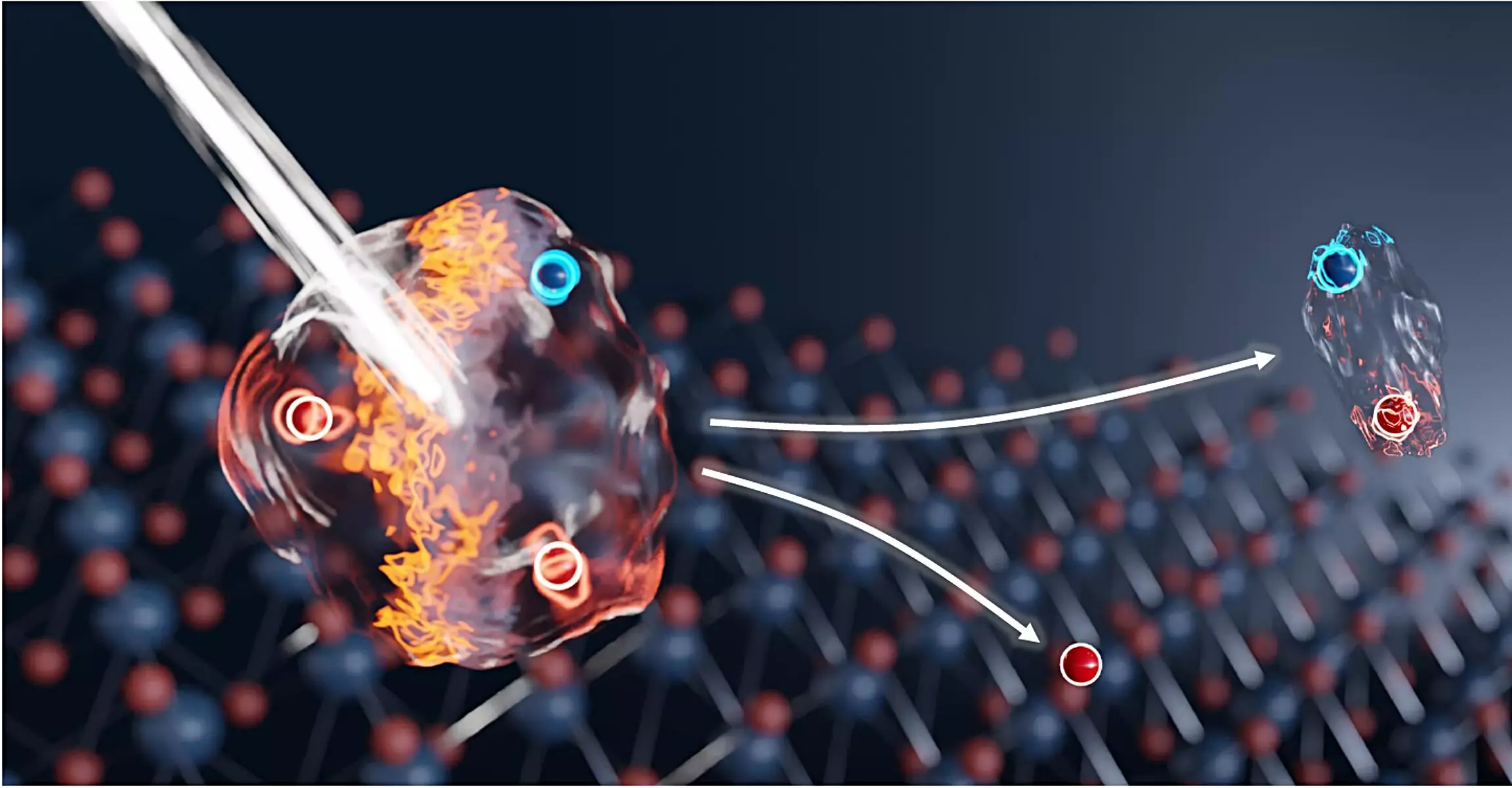
At the heart of the research lies the phenomenon of exciton formation, a binding effect between excited electrons and the positively charged holes they leave behind. When an electron in a semiconductor absorbs energy, it jumps to a higher energy state, leaving a hole that corresponds to its absence—a positively charged entity. Together, this electron-hole pair forms an exciton. Moreover, if another electron interacts closely, a trion, which is a three-particle construct, emerges. This unique coupling of charge carriers and luminescent behavior of trions presents innovative approaches for simultaneously managing both electronic and optical processes. The prior challenge for researchers had been the slow switching between these two states; however, this new study has considerably accelerated that transition.
Led by Professor Alexey Chernikov at TU Dresden, the collaborative project took advantage of specialized facilities at Helmholtz-Zentrum Dresden-Rossendorf (HZDR). This study utilized the FELBE free-electron laser to generate intense terahertz pulses, allowing for rapid experimentation with molybdenum diselenide—the material of choice. By projecting short laser pulses onto this ultra-thin material at cryogenic temperatures, excitons were created almost instantaneously. The real breakthrough occurred when researchers successfully transitioned these excitons into trions and back at record speeds, breaking the exciton-electron bond in picoseconds.
Dr. Stephan Winnerl highlighted the significance of this achievement, explaining that the manipulation of excitons and trions was accomplished through a precise frequency match using terahertz pulses. This allows researchers to toggle between the two states almost 1,000 times faster than achieved by previous electronic methods. Such rapid transitions not only enhance the understanding of quantum states but also stand to revolutionize the potential applications in various technology sectors.
The ramifications of this research extend far beyond theoretical knowledge. The rapid switching mechanism documented opens pathways for exploring complex electronic states and leveraging these phenomena in practical applications. For instance, the advancement may allow for the creation of sophisticated modulators capable of high-speed data processing. The combination of ultra-thin crystals with this novel switching methodology provides a robust framework for developing electronic components that can control optically encoded information with unprecedented efficiency.
Further prospects include enhancing sensor technologies and imaging practices. The research team suggests that leveraging the demonstrated switching actions in atomically-thin semiconductors could pave the way for versatile terahertz detectors and cameras. These devices could feature extensive pixel arrays capable of operating across a broad frequency spectrum, providing a powerful tool for capturing terahertz radiation—a critical area of interest in both scientific and industrial applications.
The transformative approach employed in this research sets the stage for an exciting future in the realm of quantum materials. Innovations stemming from this study could lead to breakthroughs across numerous fields, including communication, data storage, and sensor technology. This research shows that the interplay of excitons and trions can yield practical tools with enhanced capabilities, marrying the realms of optical and electronic engineering in ways previously thought unattainable. As the implications of these findings settle in the scientific community, it is clear that we stand on the cusp of a new era—one where the potential of two-dimensional materials can be fully harnessed to reshape technology as we know it.

